Cross Section Testing Services for PCBs and Components


What is PCB Cross-Section Testing?
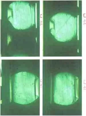
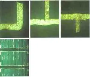
PCB cross-section testing, also known as a microsection test, inspects the internal structure of printed circuit boards for quality control and failure detection. This test is conducted by cutting a small sample of the PCB, mounting it in epoxy, and then polishing it for a cross-sectional view of the internal layers. It validates manufacturing quality and looks for defects, such as:
- Voids and cracks
- Delamination
- Inner-layer shorts and opens
- Poor plating and adhesion
- Resin recession and separation
Need to conduct cross-section tests on your printed circuit boards, components, or assemblies? Contact us for more information.Contact Us
Why is Cross-Section Analysis Essential to PCB Quality?
Cross-section analysis checks the quality of produced printed circuit board assemblies, parts, and components, before, during, and after production to identify and prevent potential failure points. With cross-section testing, Plasma Ruggedized Solutions ensures the highest possible quality of your assemblies and components through destructive testing methods, removing a small “test coupon” sample from the PCB to check multiple attributes that determine the product’s overall quality.
This test can be conducted at any point in the manufacturing process, including prototyping stages or after assembly, to test components for thermal stress and proper solder connections. In failure analysis microsection testing, we check various factors to determine the cause of product failure. Cross-section testing is the second most common test method for determining product quality after manufacturing, and offers an array of applications within the industry.
Cross-Section Testing Services from Plasma Ruggedized Solutions
Plasma Ruggedized Solutions demonstrates a commitment to quality assurance, including policies and procedures aimed at delivering high-quality conformal coating and testing solutions to meet your needs. Our microsection testing capabilities can detect any number of flaws in PCBs, ensuring that they were built to proper specifications and identifying various issues, including dielectric concerns, appropriate material selection, and even sharpness for the drill bits used in assembly manufacturing. Cross-section testing can be used for printed circuit boards, as well as for determining problems or potential flaws in smaller, individual components.
Different Levels of PCB Cross-Section Testing
For visual inspection and microsection testing, we offer three different levels for an ideal service solution to match your requirements. With our testing laboratory in California, our experts can provide results in less than one day, depending on the x-ray inspection method chosen. Our cross-section testing services are designed to determine potential defects and find possible flaws in your product from the initial stages of manufacturing, saving you time and money in the final process.
Level 1: Quick Check Cross-Section Testing
A simple cross-section testing process, level one testing services can identify the most common modes of failure in PCB manufacturing. We utilize this quick check procedure to test the results of in-house edge-back processes, and provide same-day or 1-day return of test results of your products, inspecting for the following defects:
- Nail heading
- Delamination
- Resin recession
- Copper thickness
- Laminate voids
- Lifted pads
- Registration
- And more
Level 2: In-Depth Microsection Testing
This level of cross-section testing offers more comprehensive inspection to check assemblies and components for common failure points. It is more intensive than quick check testing. However, the additional time and cost required allow us to give you a complete report of any possible problems with your PCB, including an assessment of positive design aspects and industry compliance. Level 2 testing determines if your PCB is affected by:
- Dielectric spacing
- Inner layer copper thickness
- Trace widths
Level 3: Advanced Cross-Sectional Analysis
With advanced cross-sectional analysis, we can evaluate for exact and high-level flaws, including thermal stress and other related parameters. This is a highly involved process that requires additional preparation, achieving a turnaround time of 2-3 days with a higher cost that is negligible compared to the amount of time and money that can be saved in manufacturing and failure-related costs.
Additional PCB Testing and Inspection Services
Plasma Ruggedized Solutions offers a variety of PCB testing and inspection services to ensure finished products and component materials demonstrate superior quality and functionality. Designed to check for any possible problems that may occur with your products, our testing capabilities are compatible with coated, potted, and encapsulated products.
We offer two-dimensional X-ray diffraction testing for a multi-layer analysis of printed circuit boards and BGA underfill to diagnose any potential flaws or defects, as well as ionic testing to validate components for conductive contaminants prior to conformal coating services.
Contact Us for Cross-Section Test Services to Ensure the Quality of Your PCBs
As a leading conformal coating provider, Plasma Ruggedized Solutions operates a testing laboratory in California to inspect finished products and components for quality and functionality requirements, including cross-section tests. With destructive testing methods during initial manufacturing, you can ensure your products operate as intended and feature no defects, saving you time and money throughout the process. Contact Plasma Ruggedized Solutions to discuss your requirements or request a quote to get started.Contact UsPlasma
Ruggedized


- CMMC Level 2 Compliant
- Missile Defense Agency (MDA) Certified
- NASA 8739.1A Certified
- NADCAP Electronics Certified


