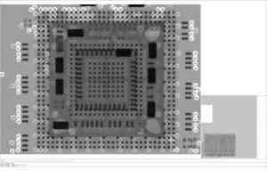
Two-Dimensional X-Ray Diffraction Testing Services
Two-dimensional X-ray diffraction, also referred to as Automated Optical Inspection (AOI), utilizes X-rays to inspect PCBs and assemblies for solder joint defects and open or short circuits that cause product malfunction. Early detection of these issues through multi-layer analysis can help manufacturers optimize subsequent processing steps and are an essential part of the overall quality check process.
There are several causes of solder voiding including the presence of too much flux in the solder paste, insufficient soak zone time during the reflow process, or solvent in the flux failing to vapor out. Since solder joint voids and other issues can’t be detected manually, a multi-layer analysis is used to test the quality of components throughout the production process to ensure well-built components and assemblies.Contact Us
Solder Joint Integrity Inspection for Improved Manufacturing
With PCBs and BGAs getting smaller in size as technology continues to advance, it is crucial to have effective processes in place for solder joint integrity inspection. Discovering issues early on in the process will prevent defective components from being used in production, improving the quality of your products. X-ray inspection is especially necessary for high volume production runs where PCB defects can result in costly product quality issues.
While it is often difficult to entirely avoid solder voiding, conducting a multi-layer analysis of your BGAs is a useful preventative measure for detecting solder joint defects that cause electronic components to short out or fail. Three areas typically inspected during x-ray diffraction analysis: the heel, toe, and fill-in. The use of specialized software and visual inspection of the X-ray helps detect voiding and micro voiding as well as:
- Inspecting BGA components for opens and shorts
- Locating solder balls that are not uniform in size, which is indicative of issues with how well the PCV is attached to the substrate
- Identifying lifted pins, misplaced parts and the presence of solder debris that can cause electric components to short out or fail
- Detecting cracks or voiding in the encapsulant
- Determining the location of through-holes in a PCB
The Importance of X-Ray Diffraction Analysis for PCB Assemblies
Plasma Ruggedized Solutions performs two-dimensional x-ray diffraction testing for PCBs and other devices. This inspection process helps find flaws and potential flaws in circuits and circuit assemblies and can help determine if the tested products meet required industry standards.
X-ray diffraction analysis allows us to inspect internal pathways and electrical circuits that are inaccessible for visual inspection. Plasma Ruggedized Solutions has specialty equipment with magnification capabilities up to 16X, to help us check for open and short circuits and a variety of other possible flaws within the circuitry of the device.
This circuit board testing procedure can also be used to determine overall quality. We can check the alignment of drilled holes with their associated circuit pads, visually inspect internal wiring and soldering connections, and many other factors. Two-dimensional x-ray diffraction testing can also be used to perform failure analysis on damaged or inoperative devices.
Contact Plasma Ruggedized Solutions for Two-Dimensional X-Ray Diffraction and Other Services
Contact Plasma Ruggedized Solutions today to learn more about our two-dimensional x-ray diffraction testing.Contact Us
Plasma
Ruggedized


- CMMC Level 2 Compliant
- Missile Defense Agency (MDA) Certified
- NASA 8739.1A Certified
- NADCAP Electronics Certified


